Sputtering Targets (1)
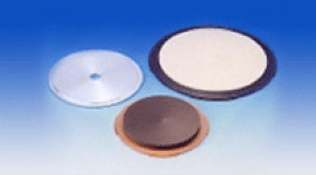
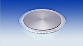
As semiconductor devices continue to shrink in size and increase in density, demand Increases for high purity, low particle films such as wiring, gate electrode, and barrier metals.We draw on our proprietary technologies to meet these needs and to further apply these technologies to the high power sputtering target market.
-
a Particle levels and bottom
coverage are significantly
improved By controlling
the re-crystallization
and the orientation of the target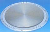
-
We offer high quality
Ti-W targets with high density
and Low particles as a refiner
of high purity tungsten

-
We provide high purity and fine
grain size dielectric, PZT,
chalcogenide and BST sputtering
targets which are prepared by our
exellent powdering and sintering
technique, applicable to new non-volatile
memory such as FeRAM, PCRAM,
and thin film condensers.

-
High purity nickel and cobalt targets
have fine, homogeneous grain size and
low magnetic permeability.

Sputtering Targets (2)
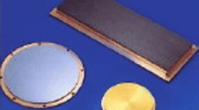
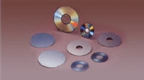
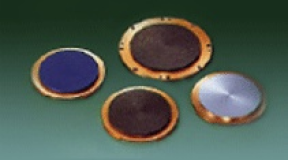
Thin films are used in various fields of modern society. It is sputtering targets which are essential for the formation of thin films. Mitsubishi Materials Corporation supplies sputtering targets of every variety which are used in each field of semiconductor,LCD,disks for optical memory and magneto optical memory,sensor magnetic disk,functional glass,superconductor and so on as a general target manufacturer.
Semiconductor devices and recording media devices, which support today's information society, have especially made great progress. Our sputtering target is improves those technique and development by utilizing real demanded quality and speed.
We consider the sputtering target business to be the general business which integrate materials,film forming and evaluation.We are going to meet customer needs which become more and more complicated and sophisticated by reinforcing and encouraging the integration with the reinforcement of each basic technique.
Applied field
- NEW TiW Target
- Optical and Magneto optical memory
- Semiconductor
- Display
- Functional Film
- Materials
- Sputtering Technique
- Film Evaluation
반도체
We supply the targets corresponding to high purity, low particle and high sputtering power for each film forming of semiconductor devices which become to be higher-integration and finer more and more. We can also supply large-size targets corresponding to large-diameterizing of wafer (300mm).
Especially dielectric materials (high dielectrics and ferroelectrics) including those electrode materials provide the best materials for each thin film forming method putting MOCVD materials and sol-gel liquid together. In addition, we invest our energy in the development of materials for nonvolatile phase change memory for the next generation putting our technology of phase change materials which we improved with rewriting disks.
Product list
| Product | Component | Purity | Characteristics |
|---|---|---|---|
| Aluminum target | Al, Al-Si, Al-Cu, Al-Si-Cu, Al-Cu-Ti, etc. | 5N | High purity and fine grain size
Low (U, Th 1ppb) |
| Silicide target | WSi, MoSi, TiSi, etc. | 5N | Low particle by fine grain size
High purity by a unique reduction method |
| Titanium target | Ti (Solder bonding, Diffusion bonding, one-body) |
4N5 6N |
Low particle by fine grain size |
| High melting point metallic target | TiW, W, Mo, Ta, Ru, Pt, Ni, Co, etc. | 4N 5N |
High purity and high density |
| Silicon target | Si, B-doped Si, P-doped Si | 5N | Large diameter (~¢13)
crystal |
| Copper target | Cu | 6N | High purity by original refining technology |
| Ferroelectric target | BaSrTiOx, PbZrTiOx, BaTiOx, etc. | 5N | Uniform mophology by high speed sputtering and low leak electric current |
Typical impunity data of Titanium target
| Purity | Fe | Ni | Cr | Al | Cu | Sn | Nav | K | U | Th | C | O |
|---|---|---|---|---|---|---|---|---|---|---|---|---|
| Ti (4N5) | 4 | 2 | 0.2 | 0.6 | 0.7 | 0.3 | <0.01 | <0.01 | <0.05 | <0.05 | 20 | 250 |
(Unit : mm)
-

Grain structure (FGR : Fine Grain Recrystalized)
Typical impunity data of Ru target
| Purity | Fe | K | Ca | Mg | Fe | Ni | Cr | Al | U | Th | density |
|---|---|---|---|---|---|---|---|---|---|---|---|
| Ru (4N) | 2 | 9 | 8 | 2 | 8 | 0.2 | 0.4 | 3 | <1 | <1 | <=95% |
(Unit:ppm, U, Th:ppb)
morphology of Ru type film
-
Ru metal fillm
-

Ru02 film
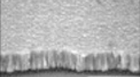
Cross sectional SEM picture of BST film on Ru electrode
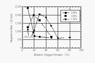
Oxygen pressure and the deposition rate
Typical impurity data of Cu target
| Purity | Fe | Ni | Si | Al | S | Ag | Na | K | U | Th | C | O |
|---|---|---|---|---|---|---|---|---|---|---|---|---|
| Cu (6N) | 0.04 | <0.01 | 0.1 | <0.05 | 0.1 | 0.3 | <0.05 | <0.05 | <0.01 | <0.01 | <0.2 | <1 |
(Unit:ppm)
Ferroelectrics targets
We have the system to supply sol-gel liquid and materials for MOCVD besides sputtering targets as materials for ferroelectrics film forming, in order to support development and mass production of ferroelectrics films for next generation synthetically.
Typical impurity data of BaSrTiO target
| Na | K | Mg | Al | Cr | Mn | Fe | Co | Ni | Cu | U | Th | |
|---|---|---|---|---|---|---|---|---|---|---|---|---|
| 4N | 8 | 3 | 3 | 9 | 1 | <1 | 3 | 1 | 1 | 2 | - | - |
| 5N | 1 | <1 | <1 | <2 | <1 | <1 | <1 | <1 | <1 | <1 | <1 | <1 |
(Unit:ppm, U, Th:ppb)
Electrical data of BaSrTiO film
| Target purity | Specific dielectric constants | tan  |
Leak electric current for 1V |
|---|---|---|---|
| 4N | 216 | 0.0164 | 9.90E-09 |
| 5N | 205 | 0.0151 | 6.94E-09 |
By (Ba0.5Sr0.5) TiO3- target
BSEM photo of BaSrTiO film
CHART
-
SEM photo of BaSrTiO film
-
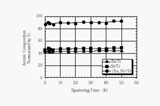
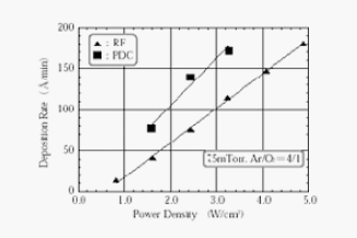
Composition for sputtering time (BST target)

