Wafer Coating and MOD Liquids
-
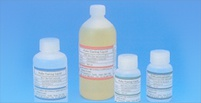
We have developed Sol-Gel and MOD solution for forming ferroelectric and high permittivity thin films by Spin-coating method.
Sol-Gel solution
•Sol-Gel liquid which enables to form dielectric thin film easily.
•Sol-Gel Solution for FeRAM
•You can get More Uniform and Thinner Films by Lower Annealing Temperature
• Surface morphologies of PZT films
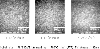
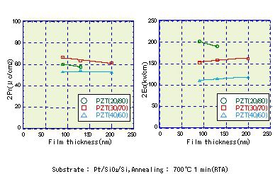
•Properties of PZT thin films
- Films with good saturation characteristics
- Film thickness down to 90nm without degradation of properties
- Low drive voltage
•Low temperature preparation of PZT films (450℃)
You can get films with 2Pr > 20.
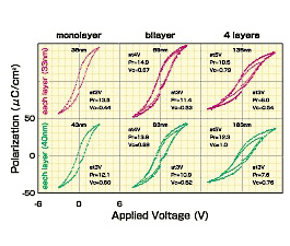
•Low temperature preparation of SBT films (650℃)
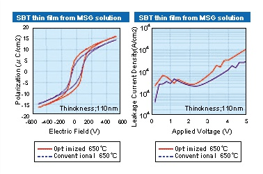
- * Optimized 650 is Symetrix's proprietary process You can easily prepare SBT films by Modified Sol-Gel Solution using low temperature annealing
- 1 ㎛ 두께가 넙는 필름 대상의 PZT 졸겔 용액
- 1회 코팅으로 최고 1 ㎛ 두께의 PZT 필름을 얻을 수 있다!!
-
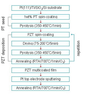
•Preparation of films
-
•Uniformity of film thickness

-
•Microstructures of single-coated films

You can get film with excellent uniformity of thickness
-
•Microstructures of multicoated films

-
•Polarization and longitudinal strain hysteresis loops for multicoated films

-
• Good properties on each film
• Choose the thickness you hope for your application.
-
•Densification of PZT thick film
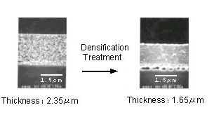
• You can easily get dense film by densification
• The film is expected for low leakage current density
-
• ETC

• PZT, PLZT – (Pb, La)(Zr,Ti)O3
• SBT, SBTN – SrBi2(Ta, Nb)2O9
• BST – (Ba,Sr)TiO3
• LSCO – (La,Sr)CoO3
• BLT, BIT – (Bi,La) 4Ti3O12
• BSO – Bi2SiO5
* We can also produce other solutions and solutions
with dopants, Please feel free to ask us.
MOCVD source
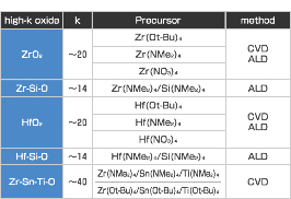
•MOCVD source, which enables a high step coverage film
|
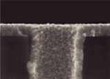
Conventional deposition methods such as sputtering and CSD are limited when applying devices with fine and multilayered structure for higher integration and higher speed operation. By comparison the MOCVD method has good coverage for fine and complicated substrate. Mitsubishi Materials Corporation has been developing metallo-organic compounds for MOCVD and MOCVD sources for liquid delivery system. |

|
|---|
MOCVD is an ultimate film deposition technology.
We will support the next-generation semiconductor device from the viewpoint of user
TARGET |
We proceed the development of MOCVD materials for the next.
|
|---|---|
ADVANTAGE |
Distinction in materials, positive tie-up with device / process machine manufacture and the reliable supply system. |
•Capacitor and electrode for memory device
Relationship between integration density and deposition method

•Capacitor and electrode for memory device
Relationship between integration density and deposition method
